Schema A Pcb Altium Designer
Altium schematics fiverr screen Altium pcb-project: tutoriel français 3 schematic Altium routing progettazione differential stack circuit regole rules avoiding considerations tolerance violations componentes montaje tuning autorouter multilayer interfaccia conto router
Altium designer PCB designing tutorial step by step guide
Design schematic and pcb in altium by wangdegang Altium pcb Design schematics and pcb in altium by faiz07
Come creare un layout pcb partendo da uno schema in altium designer
Getting your layer stack rightAltium fiverr Pcb altium tutorial schematic update designer document select1 hour tour about altium designer(schematic-pcb designing).
Design pcb schematic and layout in altium by sociallyveganAltium designer reviews 2021: details, pricing, & features Altium designer pcb designing tutorial step by step guideAltium designer pcb designing tutorial step by step guide.
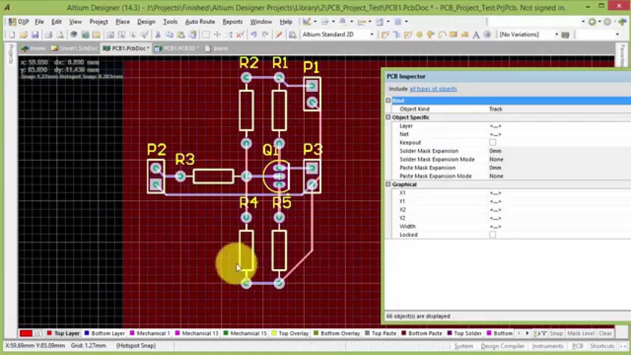
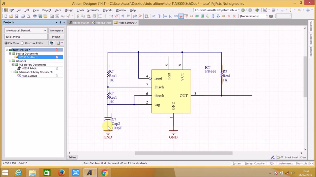
![Come creare un layout PCB partendo da uno schema in Altium Designer](https://i2.wp.com/www.windowsblogitalia.com/wp-content/uploads/2019/09/pcb.png)
Altium schematic
Pcb schema circuito diagramas elettrici partendo altium motherboardAltium pcb Altium designer pcb design tutorialAltium pcb schematic screen fiverr.
.
![Design schematics and pcb in altium by Faiz07 | Fiverr](https://i2.wp.com/fiverr-res.cloudinary.com/images/t_smartwm/t_main1,q_auto,f_auto,q_auto,f_auto/attachments/delivery/asset/042714782a81a45d93d3005cfceb1748-1595361908/Circuit_bb/design-schematics-in-altium-designer.png)
![Design pcb schematic and layout in altium by Sociallyvegan | Fiverr](https://i2.wp.com/fiverr-res.cloudinary.com/images/t_main1,q_auto,f_auto,q_auto,f_auto/gigs2/112772182/original/dc3bd3b891d1f9e551c694c9a40367b1722924bd/design-pcb-schematic-and-layout-in-altium.jpg)
![Getting Your Layer Stack Right | Whitepaper | Altium](https://i2.wp.com/www.altium.com/resources/styles/doc_import/public/doc-import/yGZ4_rsjMRxmPnYvrkTwRmqASdcjMK6x0VrWe4VKO3uJNzIuLnVDJ7vXAD1pGHliWdaqEoODBep5RGRfAwYaF12b_K4lrcujd7RCzqf87xSop8tHrbUvoruBfBPPCz76VbZ1ZpHX.png?itok=Y6wki668)
![1 Hour Tour about Altium Designer(Schematic-PCB Designing) - YouTube](https://i.ytimg.com/vi/GBk0q3IofNI/maxresdefault.jpg)
![Altium Designer PCB Design Tutorial | PCBCart](https://i2.wp.com/www.pcbcart.com/Uploads/Editor/2016-08-09/57a995846c905.jpg)
![Altium designer PCB designing tutorial step by step guide](https://i2.wp.com/microcontrollerslab.com/wp-content/uploads/2017/09/Altium-pcb-designing-step-3.jpg?ssl=1)
![ALTIUM PCB-Project: tutoriel français 3 Schematic - YouTube](https://i.ytimg.com/vi/EHmMXPkllDc/maxresdefault.jpg)
![Design schematic and pcb in altium by Wangdegang | Fiverr](https://i2.wp.com/fiverr-res.cloudinary.com/images/t_main1,q_auto,f_auto,q_auto,f_auto/gigs/181005974/original/40bd490e13f0e0cf055bfb7f4d3bfdfa958486c7/design-schematic-and-pcb-in-altium.png)
![Altium designer PCB designing tutorial step by step guide](https://i2.wp.com/microcontrollerslab.com/wp-content/uploads/2017/09/Altium-pcb-designing-step-2.jpg?ssl=1)
![Altium Designer Reviews 2021: Details, Pricing, & Features | G2](https://i2.wp.com/images.g2crowd.com/uploads/attachment/file/181210/PCB-Layout-1.png)