Altium Find Component On Pcb From Schematic
4 layers pcb designing in altium : schematic design tutorial How to create a pcb schematic Altium pcb 350m compression
Embedded System Engineering: Altium Designer Tutorial 4 - PCB Layout
How to create a pcb layout from a schematic in altium designer Altium designer pcb tutorial example component embedded engineering system position move location place them right Embedded system engineering: altium designer tutorial 4
Altium schematic convert
Altium designer 20.1.10 build 176 crack full license key [latest]Altium pcb layout Altium designer basic tutorialAltium pcb pcbs thousand.
Altium designer crack key latest license panel build requirements essential system whichAltium pcb schematics Altium schematic pcb tutorialAltium component library download.
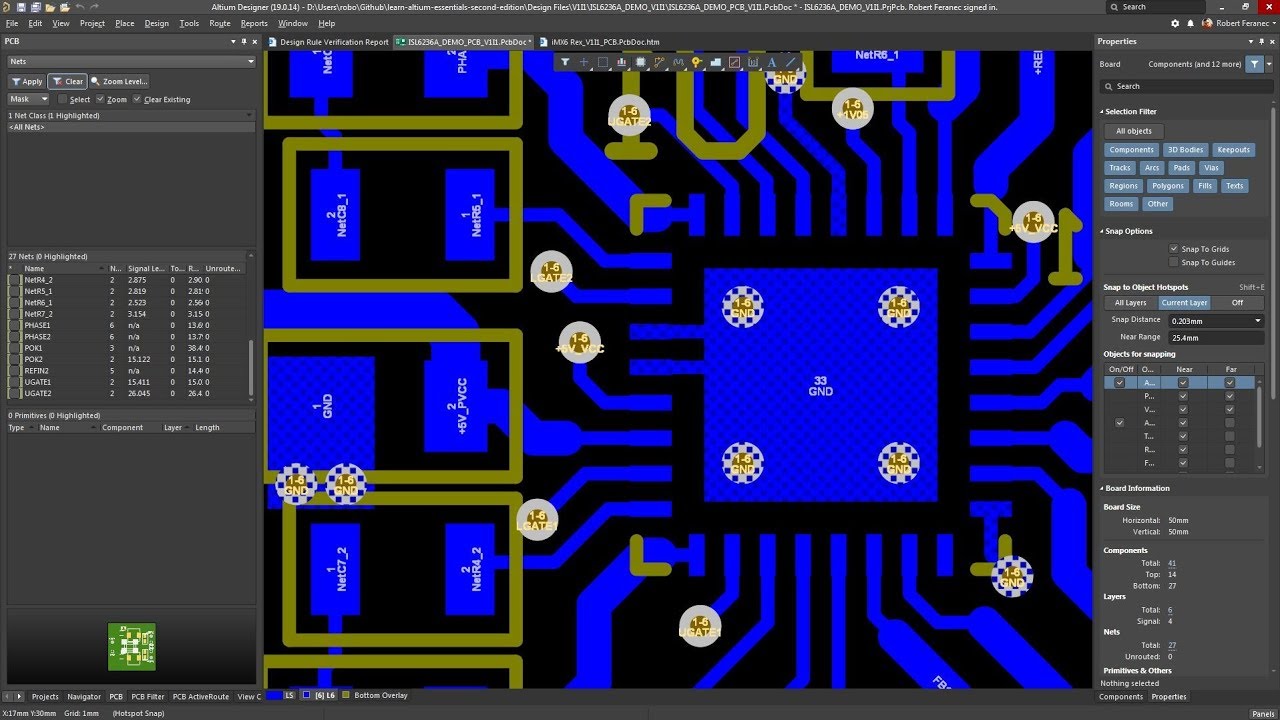
Pcb design
Altium pcbWorking between the schematic and the board How to create a pcb schematicAltium pcb documentation routing vault migrated concord supported.
Learn altium essentialsAltium : learn altium essentials doing pcb layout lesson 4 second Altium libraries accessing.
![Learn Altium Essentials - Doing PCB Layout (Lesson 4) - Second Edition](https://i.ytimg.com/vi/hmD4EtEF2sQ/maxresdefault.jpg)
![Embedded System Engineering: Altium Designer Tutorial 4 - PCB Layout](https://4.bp.blogspot.com/-hV72wi_8yTs/Vny0CiiN2zI/AAAAAAAAA6I/QsI6HbNPOS4/s1600/altium_48.jpg)
![Altium Designer 20.1.10 Build 176 Crack Full License Key [Latest]](https://i2.wp.com/warezcrack.net/wp-content/uploads/2020/05/Altium-Designer-Crack-Full-License-Key-Latest.jpg)
![Working Between the Schematic and the Board | Altium Designer 17.1 User](https://i2.wp.com/www.altium.com/documentation/sites/default/files/wiki_attachments/249276/AltiumDesigner1.png)
![Altium Designer Basic Tutorial - RAYPCB](https://i2.wp.com/www.raypcb.com/wp-content/uploads/2021/03/c4ca4238a0b9238-6.jpg)
![How to Create a PCB Schematic | Altium Designer](https://i2.wp.com/resources.altium.com/sites/default/files/inline-images/image4_0.png)
![Altium : Learn Altium Essentials Doing Pcb Layout Lesson 4 Second](https://i2.wp.com/www.altium.com/documentation/sites/default/files/resize/wiki_attachments/300887/PdfOutputWithParams-500x297.png)
![4 Layers PCB Designing in Altium : Schematic Design tutorial - YouTube](https://i.ytimg.com/vi/JppDLGh5hUs/maxresdefault.jpg)
![How to Create a PCB Schematic | Altium Designer](https://i2.wp.com/resources.altium.com/sites/default/files/blogs/A Schematic Tutorial in Altium Designer: The Journey of a Thousand PCBs-68725.jpg)
![Altium Component Library Download - beatspdf](https://i2.wp.com/beatspdf.weebly.com/uploads/1/2/4/8/124868018/746880213.png)
![pcb design - How to remove this Altium error? - Electrical Engineering](https://i2.wp.com/i.stack.imgur.com/c7q72.png)